A-Laser PCB Depaneling
A-Laser partners with you as we navigate today’s modern world of electronic devices.
All of us are surrounded by various technologies day and night and we want to be your go-to manufacturer in the latest technology production.
Think of all the devices we use in a day: our phones, our TVs, the computers we work on; the systems in our cars deploying the airbags or medical components that save lives. All of these technologies have one thing in common – they all have printed circuit boards (PCBs) hidden somewhere inside the design.

What is PCB depaneling?
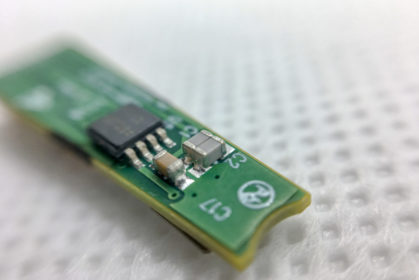
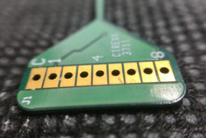
PCB depaneling is the process of removing numerous smaller, individual boards from a larger panel during manufacturing.
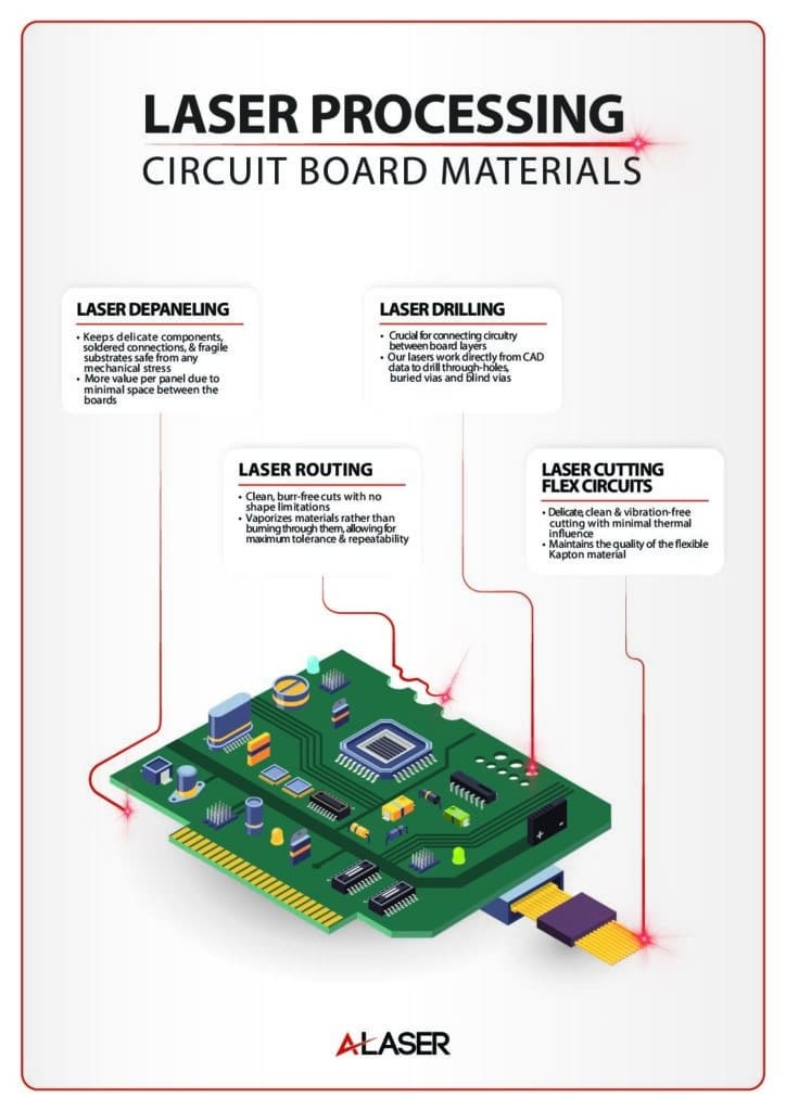
The laser process used keeps delicate components, soldered connections, and fragile substrates from any mechanical stress. Due to minimal space between the boards, there is more value per panel. In addition, components can be placed adjacent to each other to minimize unnecessary bulk and weight.
PCBs are usually manufactured in large panels with multiple boards, but can also be produced as single units. The depaneling process can be fully automatic, semi-automatic, or manual. This brings lower throughput, along with eliminating the added cost of tooling and waste removal associated with mechanical methods.
Why are PCBs Important?
Without PCBs, recent electronic designs would not have been possible. These marvels of technology support and connect all the electronic components needed to make the magic happen inside a device or machine.
The miniature design of various devices that require printed circuit boards is pushing the limits of electrical performance.
With continued advances in integrated circuit (IC) fabrication, the number and density of connections to interface the devices continue to rise.
In order to further aid in the increased output of PCBs while still maintaining a small size, depaneling was created.
Typical Depaneling Methods
What the Numbers Say:
In every one of the above methods, except in laser routing, some degree of mechanical stress is exerted on the boards. This inflicted stress can lead to delamination or cause a space to develop. These methods also require that the final connections between the boards and panel be removed. The bending stress can damage components close to the areas of necessary removal.
Laser routing, which is part of the laser etch PCB processes, is the most recent tool in depaneling flex and rigid boards.
Laser routing offers all of the following benefits:

Temperature:
A knowledgeable and experienced operator can select the optimum settings to guarantee a clean cut with no burn marks. Material type, thickness, and condition are all factors that will be considered and will determine the speed (and consequently will affect the temperature) of the laser.
Expelled Material:
An exhaust or filter system removes any expelled material during the laser process.
If the application does produce an extremely small particle residue, compressed air or a smooth tissue can be used.
Stress:
Since there is no contact with the panel during cutting, lasers allow all most or all depaneling to be done after assembly and soldering. This allows for the avoidance of any bending or pulling of the board and therefore no stress is applied and no damage occurs.
Ready for a quote?
Why Choose A-Laser for PCB Depaneling?
Tooling expenses and expansive fixtures for die-cutting and other conventional methods is eliminated with A-Laser depaneling.
A-Laser depaneling is done with speed, pin-point accuracy, no tooling cost or wear, no part induced stress, and no cutting oils or other waste. A no-touch depaneling method using lasers provides a highly precise singulation without any risk of harming material, regardless of substrate.
The technology also works in the optimum pulse duration range for printed circuit board material processing. This pulse range plays a key role in processing efficiency and leads to lower cost and maximum use of processing time.
Reduce production costs with a fast and easy set-up.
Laser depaneling is a non-contact process, which means standard SMT carriers can be used throughout the production process. No special clamping or fixtures are needed because the only mechanical-dynamic forces acting on the boards are due to the handling equipment. Laser depaneling also is capable of processing boards with assembled components on both sides.
Our lasers cut substrates right next to delicate components without causing any mechanical stress. This allows small applications with populations right up to the edge of the printed circuit board to be expertly handled. The occurrence of discard products is also minimized due to tight tolerances.
The A-Laser depaneling system has very little waste, negating pollution in the workplace. Particles are also kept clear of the laser, which reduces maintenance frequency. The built-in exhaust system removes all the material vaporized by the laser, leaving a residue-free service.
The software in our PCB depaneling machines allows the user to operate the machine at the touch of a button. The specialized laser source and a compact, touchscreen control panel make a user-friendly system. The optimal focus of the laser beam adjusts automatically, and a security glass enclosure prevents accidents by absorbing laser reflection.
Due to the trend toward smaller and smaller components in current technology, laser depaneling meets the demands of any project. The focus spot of the laser beam is ideal for very narrow channel cuts, saving space and material.
When to Use A-Laser Depaneling
A-Laser depaneling is ideal for micromachining metals, plastics, ceramic materials, and material combinations. Some of the specific applications include drilling of microvias in HDI circuit boards, structuring of TCO/ITO, laser removal of tin-resist, drilling of flex material, the opening of solder-resist, as well as laser repair and rework of printed circuit boards.
A-Laser systems can work as a stand-alone unit or as components of fully integrated production lines.
Time-to-market & changeover times are greatly reduced
The need for complicated tools or adaptors is eliminated and only the layout data has to be uploaded. Small, sensitive PCBs with narrow spaces on the panel are ideal applications and result in increased operational capacity and better quality.
As the technology community continues to innovate and create smaller and more advanced devices, A-Laser offers the latest in precision part manufacturing to meet this demand. The reduced size and intricate design of new technology requires smaller PCBs. Since there is no standard set for PCBs, every board is design-specific. This results in the need for depaneling.
A-Laser employs laser PCB depaneling to ensure production factors such as stress, precision, and cleanliness are kept at an unparalleled industry standard. Let us work with you today to ensure the premier, most cost-efficient product.
To learn more, chat with our PCB depaneling experts here.
How is PCB Depaneling done?
A-Laser depaneling is done with speed, pin-point accuracy, no tooling cost or wear, no part induced stress, and no cutting oils or other waste. A non-contact depaneling method using lasers provides a highly precise singulation without any risk of harming material, regardless of substrate.
As the technology community continues to innovate and create smaller and more advanced devices, A-Laser offers the latest in precision part manufacturing to meet this demand.
Why Should You Consider PCB Depaneling?
The reduced size and intricate design of new technology require smaller PCBs. Since there is no standard set for PCBs, every board is design-specific. This results in the need for depaneling.
A-Laser employs every method of PCB depaneling to ensure production factors such as stress, precision, and cleanliness are kept at an unparalleled industry standard.
Let’s Get Started On Your PCB Depaneling Project
Our technical engineers walk you every step of the way through the manufacturing process. We’d be happy to talk more about your project and how we can help.
We also offer a wide range of laser-cutting services, including laser skiving, laser depaneling, laser routing, and more. We work with both UV lasers and infrared lasers to give you the choice of the best method for your project.
Simply fill out the form below to get started today.


