Precision Laser Cutting for the Semiconductor Industry Service
Trusted by
1,000’s
of Satisfied Customers
30+
Years in Business
Laser Cutting Semiconductors
The semiconductor industry makes vital components for the technologies we all depend on. The semiconductor industry is looking for faster, smaller, more powerful, intricately precise, and massively efficient processes. Ultraviolet (UV) laser cutting is a perfect fit. A-Laser’s beam can hold up to .0005″ tolerance, it can cut complex profiles, and it can easily change the required cut by altering the computer aided design (CAD) file.
Laser machines can also process a variety of materials like Polyimide (Kapton), Polyimide (Cirlex), Q-pad, and Grafoil. Processing those materials using lasers can add huge value to the overall supply chain for the semiconductor industry.
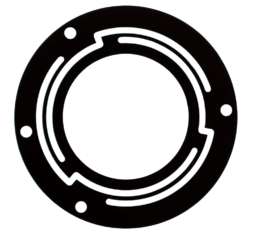
Gaskets for instance, used in semiconductor processing are vital in the production stream. The uniformity of the cut profiles for parts ranging in size from 11.500” inches OD x 9.75” ID to 19.600” ODx17.75” ID, are a requirement when used in such conditions. Tolerances held are as small as +/- .001” mil. Utilizing a beam diameter of 20um, this kerf creates well defined sharp edges, straight walls, and consistent cuts. Whether a simple or complex geometry, a shim can be vital in the functioning of mechanical devices. Requiring more durability, shims from stainless steel reinforced Grafoil, have proven to be a welcomed solution. From sizes of .250 O.D. up to 5.40 O.D., and a tolerance of +/- .001” mil is providing reliable long-term use.
Frequently Processed Materials for the Semiconductor Industry

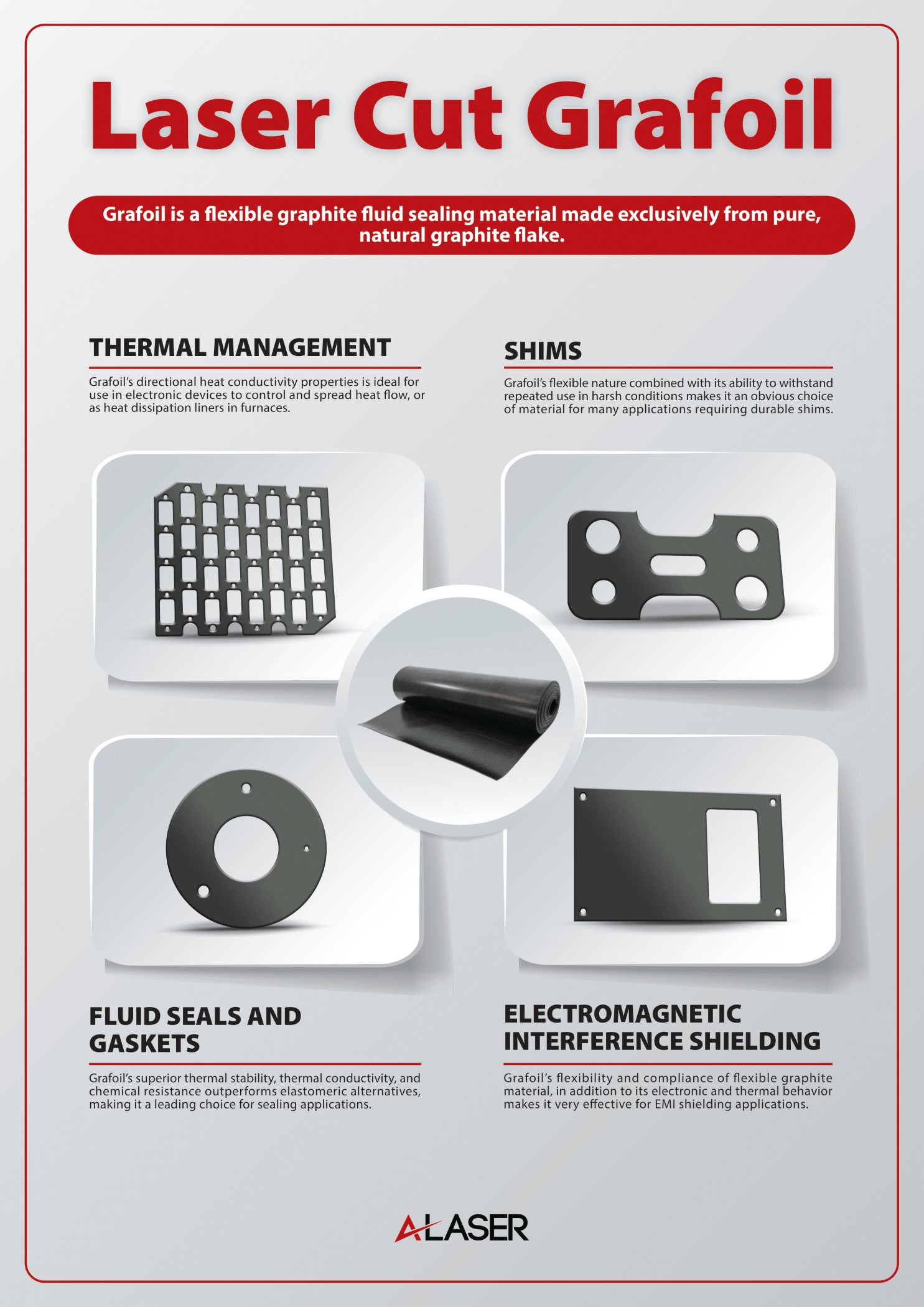
Grafoil
Grafoil® is compactable, resilient, and conformable, or compliant. It’s chemically resistant to fluids, can withstand a lot of heat and pressure, and fits snugly to any surface to prevent leaks.
Grafoil’s unique physical and chemical properties make it ideal for sealing and for high-temperature applications. The flexibility of Grafoil is due to its naturally-occurring graphite flake. The crystal structure of natural graphite consists of layered planes of carbon atoms with bonding between the planes. This structure leads to the electrical, thermal, and mechanical differences in the conventional properties of graphite and explains its natural lubricity.
Q-Pad
Q-pad, for example, is a composite of silicone rubber and fiberglass. What makes this material special is its outstanding mechanical and physical attributes, which makes it ideal for many applications.
Q-pad materials vast application possibilities are due in part to its flame retardant characteristics. This makes it ideal to be used to electrically isolate power sources from heat sinks. It can be applied between a transistor and a heat sink or between a heat sink and a chassis. Q-pad, then, is excellent under electrically isolated power modules, in gaskets, or in devices such as resistors, transformers and solid state relays.
Q-pad also has:
- Thermal impedance: 1.13°C-in2/W (@50 psi)
- Thermal Conductivity 0.9 W/mK
- Maximum Usage Temperature

In addition, there are many physical advantages to using the Q-pad material. Q-pad is easy to handle and can be installed prior to soldering and cleaning. It conforms to surface textures and eliminates processing constraints associated with grease.
Laser cutting can improve both quality and efficiency, and its use in processing Q-pad proves it. Lasers provide the best software-controlled beam quality. Engineers can design the drawing and the laser will give them the freedom to request tight tolerances and precise cuts.
Why Use A-Laser for Your Semi-Conductor Material Needs?
At A-Laser, offering the latest UV laser technology to meet semiconductor demand is our priority. Not only do we specialize in cutting material like Q-pad, we offer an extensive variety of solutions when it comes to precision laser cutting for semiconductor industry applications. We have expert engineers at CAD, tool engineering, and process development.
A-Laser engineers will evaluate customer’s materials and recommend the best system to process them, then work with the customer to develop faster and more efficient processes.
By having an excellent engineering team, A-Laser excels in quality and especially when processing various laser cutting materials for the semiconductor industry. Recommending the best solution while having the ability to do the needed adjustment in CAD files and laser tooling are what sets A-Laser apart.
