Practical Guide: The Top 5 Benefits of UV Laser Depaneling
Printed circuit boards (PCB) have been depaneled by many PCB depaneling methods, including mechanical routers, dicing saws, and pizza cutters for decades. Changes in size, shape, material and intricacy of circuit boards require manufacturers to change with current technology needs. Just as you wouldn’t use any technology from decades ago, the equipment and methods used to make the most innovative technological devices must be upgraded as well.
Typical depaneling services and technologies are dying out and becoming obsolete for a host of reasons. New electronic components are becoming more complex and sensitive to vibration or contamination.
The answer? A-Laser UV Laser PCB Depaneling.
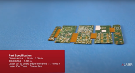
A-Laser ultraviolet (UV) systems use laser ablation to process materials, thus vaporizing material during manufacturing processes rather than melting it. Vaporizing creates a clean, burr-free edge and leaves virtually no carbon residue. It also means no vibration or mechanical stress on solder joints, a clean dust-free environment, and the ability to depanel flex circuits quickly and cleanly regardless of the stack-up.
UV laser PCB depaneling is computer-aided design (CAD) driven. Using the latest design technology allows for the immediate implementation of design changes. There is also no dulling or chipping of laser beams, which eliminates any added expense or time wasted waiting for hard tools.
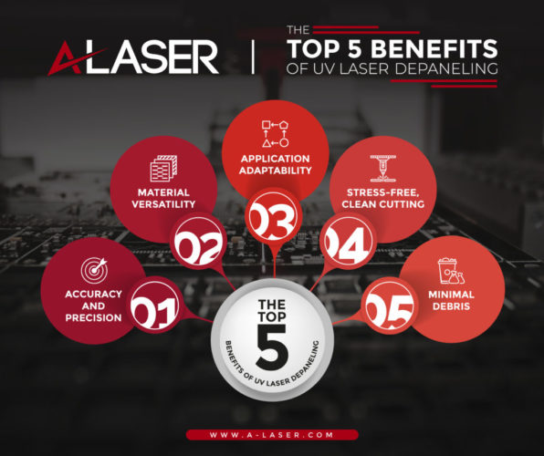
Below are the top 5 benefits to UV laser depaneling:
Benefit #1: Accuracy and Precision
The detail and accuracy of UV lasers simply cannot be matched using any other PCB depaneling method. The quality and reliability of computer-driven lasers are unequaled by any of the traditional board modification toolings.
Before the use of UV lasers, conventional laser cutting used a highly focused beam of heat and could render the board useless with one careless cut. The customary laser cut was also often jagged and uneven.
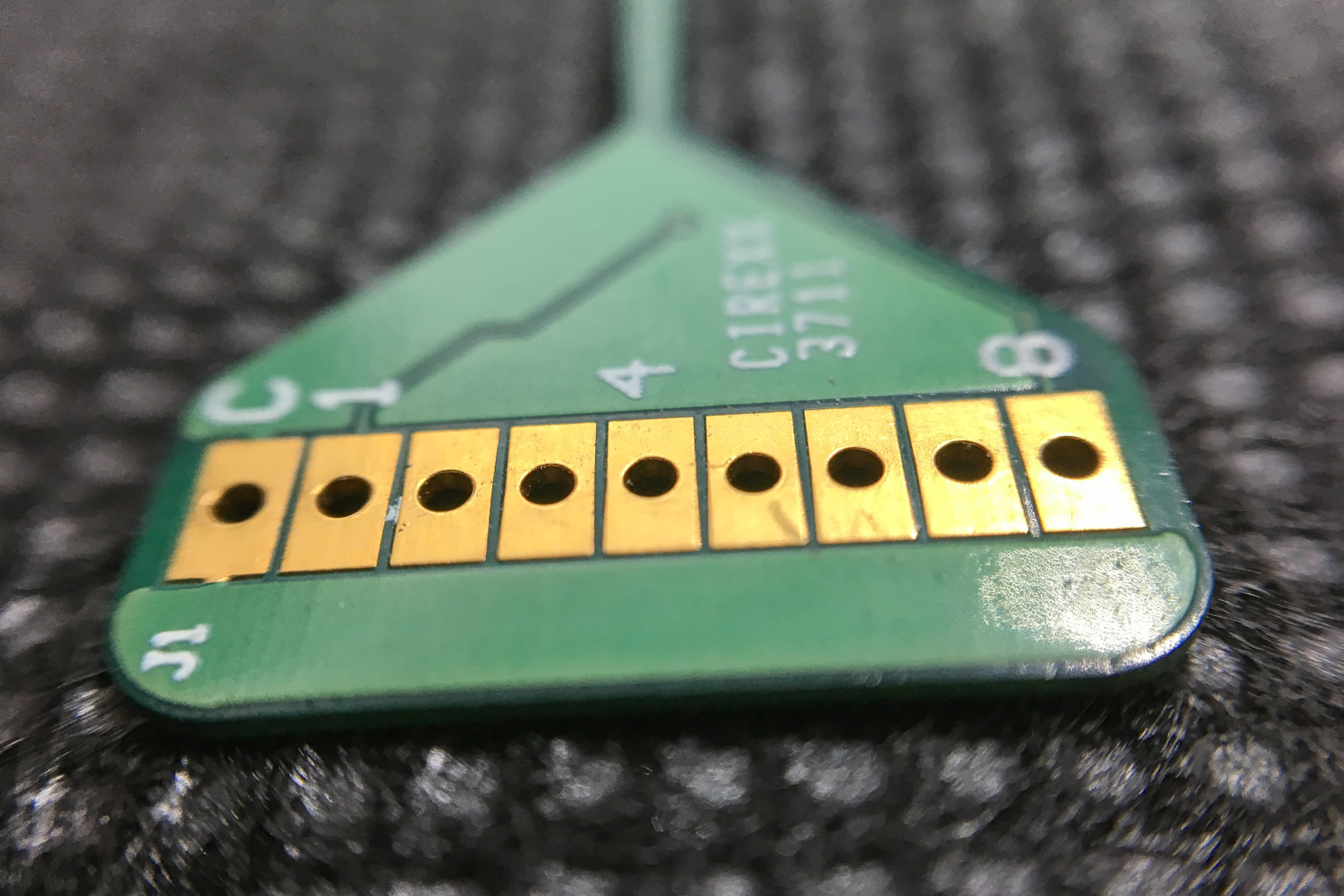
A-Laser UV laser cutting reduces the heat point exponentially, resulting in a straight, fine cut even at the microscopic level. This precision and specificity are key to deliver the kind of results that today’s technologically advanced applications require.

Benefit #2: Material Versatility
UV laser PCB depaneling can handle any material because it does not produce the damagingly high amount of heat that traditional depaneling methods create.
There is also no radiant heat with UV lasers, so there is no surround field damage from the application point of the laser.
Any project, regardless if the material ranges from very dense to extremely fragile, can be successfully completed using UV lasers because they are precise, efficient, and cost-effective.


Benefit #3: Application Adaptability
Besides drilling and cutting, A-Laser’s UV lasers can perform multiple other functions. They are ideal for skiving, serialized marking, engraving, metal ablation, microscopic routing, and more.
Miniature is the new, in-demand expectation in technology. From smart watches, to bluetooth headphones, and virtual reality goggles, smaller is the new trend. UV lasers allow this demand to be met while still producing high-capacity assembly output and yield. The extremely detailed cutting and edging UV lasers can produce is the exact type of quality today’s projects require and does not drive up the cost to the customer.
Creators and designers of today’s most advanced technology are playing with shapes and forms previously not possible due to traditional tooling limitations. UV lasers offer a constraint-free design parameter that puts A-Laser at the front of its field in UV laser depaneling and production.
Benefit #4: Stress-Free, Clean Cutting
Typical PCB depaneling methods using mechanical routing causes deformation. The stresses introduced from traditional depaneling methods include:
- Vibration
- Delamination of PCB Edges
- Debris and Dust Creation
- Cutting Friction and/or Damage
- Wiring and Circuit Damage
- Melting
- Short-Circuiting
All the traditional destructive PCB depaneling methods also require an underlay material to prevent the tool from cutting into the work surface. This greatly affects accuracy due to the need for clamping or cushioning for stability.
A-Laser’s UV lasers offer the delicacy needed for the most modern technological projects. UV lasers do not put any stress on the PCB panel during production, so the stress factors caused by outdated depaneling methods are eliminated. UV lasers will operate with:
- No Pressure Application Damage
- Stress-free PCB Cutting
- Extremely Accurate Cutting
- No Warping of Vibration
- Minimal to No Debris and/or Dust
- Little to No Over-Heating/Melting
- No Slag on Cut Edges
Benefit #5: Minimal Debris
UV laser’s ability to produce little or no debris is worth special attention. Non-laser depaneling produces a significant amount of debris that has to be vacuumed off both the board and the workspace, resulting in both an increase in production time and cost.
A router leaves a coating of dust particles on not only the panel but also can damage sensitive components. The resulting need for additional cleaning, as well as the inhalation of fiberglass dust by workers, is a major concern.
A-Laser UV lasers ablate material, producing finer particles that are extracted by the exhaust system. Any remaining, minimal debris is not damaging to the highly sensitive components.
Conclusion
UV laser PCB depaneling for extraordinary quality depaneling services is a fast-growing portion of laser cutting services. This is due to laser ablation’s high cut-quality, quick turn capability, and unmatched material handling experience.

What would your production floor look like if you were willing to introduce an A-Laser UV laser system? How much increase in profit would you achieve by offering and delivering the highest-quality products to your customers? These top 5 benefits should convince you that A-Laser’s UV laser technology is a must as your company looks to the future in the depaneling field.
