Why Semiconductor Engineers Choose Laser Over Mechanical Cutting
Laser cutting plays a crucial role across various sectors of the semiconductor industry due to its unparalleled precision, minimal heat-affected zones, and ability to process delicate and diverse materials. Engineering teams working in the industry have discovered for the past few decades the advantages of using laser technology to keep our demands for new products. This discovery comes with great responsibility to manufacturers providing services to the industry. Semiconductors are powerful devices emanating from microscopic platforms. This means every part of the supply chain must co-exist as a whole by using practices and procedures that result in accurate and precise components. Material handling pre and post laser is part of the process. With so much riding on each step, material usage is a key part. Here’s a breakdown of the kinds of materials being laser cut:
- Silicon (Si)
- Low K dielectric
- Thin Films and Adhesives
- Metal Alloys: Stainless Steel, aluminum, copper, titanium, nickel, tungsten, others.
- Plastics and Polymers: Acrylic, POM (Delrin), Polyimide (Kapton), polypropylene.
- Gasketing Materials: Graphene, other gasketing materials.
These listed materials and many more have crucial roles in the manufacturing of semiconductors. With a high demand for quality and conformance to manufacturing standards, laser technology has become a key partner for semiconductor cutting methods that other techniques cannot compete with.
Lasers Are Beaming With Advantages
Precision and quality have become a characteristic that laser service providers strive to maintain and by working with the semiconductor industry, this has assisted in achieving such high levels of performance. The advantages to semiconductor laser cutting over mechanical means such as die-cutting, stamping, or CNC machining, for crucial components gives engineers options for new designs and materials. Here are prominent advantages to why laser technology is being used for the semiconductor industry:
- Precision and miniaturization: With small beam diameters of 20 to 35 microns, intricate designs, tight radius, and sharp corners are achievable.
- Minimal heat-affected zone (HAZ): Prevents damage to delicate semiconductor structures and maintains material integrity.
- Reduced chipping and cracking: Silicon and ceramics can be brittle. Laser can adjust to prevent damage and increase yield.
- Non-contact process: Eliminates tool wear, contamination, and mechanical stress associated with traditional methods.
- High throughput: Faster processing speeds compared to mechanical cutting.
- Flexibility: Easily adapted to different wafer designs and material properties through software adjustments, supporting R&D and prototyping.
- High precision and tight tolerance: How Tight Can Tolerances Be in Precision Machining?Essential for proper functioning and alignment of complex processing machinery. Many lasers cut with a standard tolerance of +/- 0.0254mm, but can be tighter, depending on project.
- Cleanliness: Non-contact cutting minimizes debris and contamination, which is paramount in cleanroom environments.
- Versatility: Ability to cut a wide range of materials with varying thicknesses.
- Customization: Enables quick prototyping and production of custom parts for specialized equipment.
Engineering Support
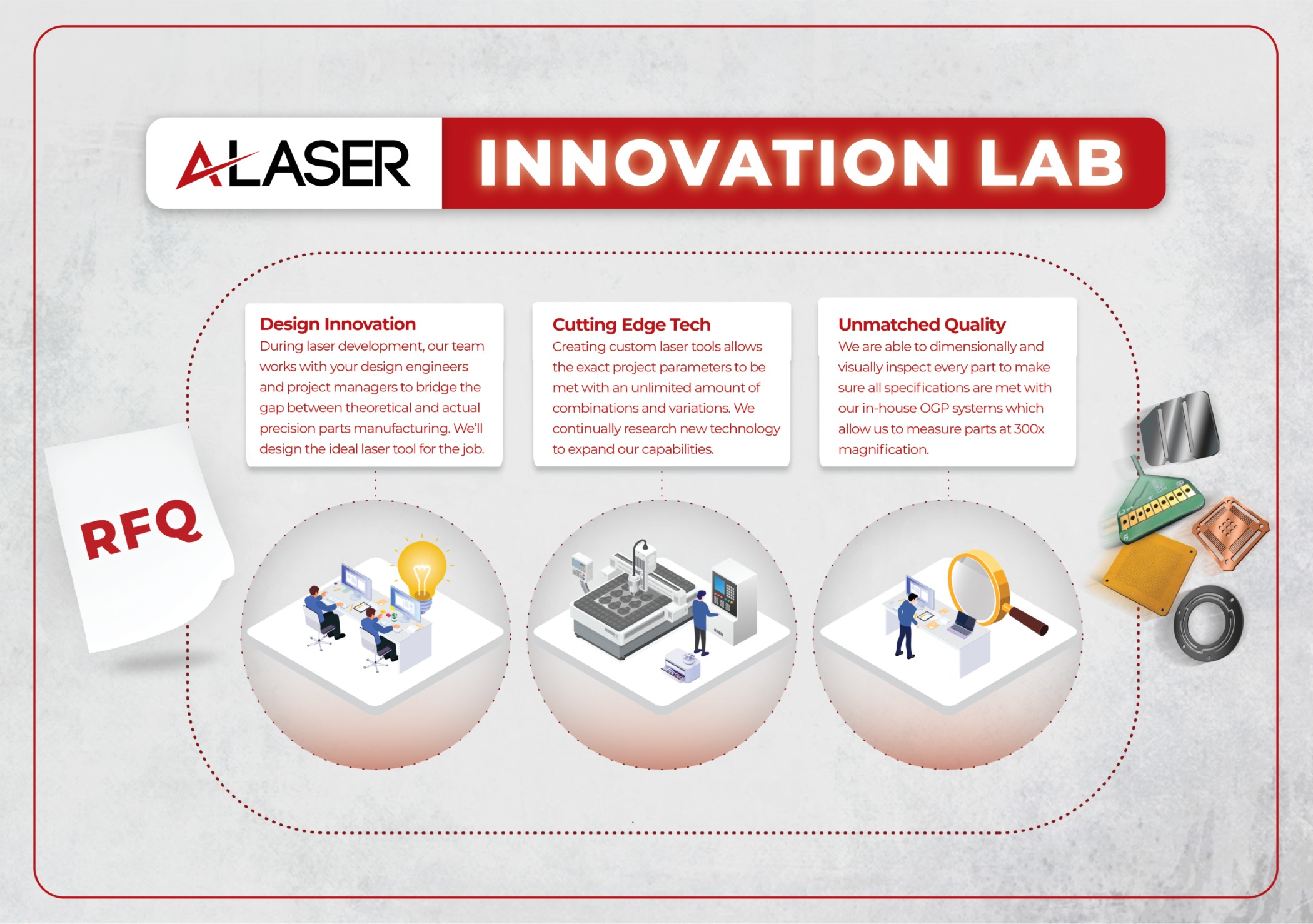
One of the best characteristics of laser technology is the ability to be flexible on the variety of materials that can be cut, but also flexibility in the processing of these precision components. Mechanical, electrical, process, and testing engineers can all use the expertise given by laser cutting specialists to take their ideas into tangible entities. Support for any project often begins with R&D and prototype projects. Laser technology has a keen advantage over many other methods that it does not incur cost for special tooling or extensive set-up. It is common for small testing stages to need just a handful of parts and gradually increase quantities as progress is made. The parameters and process are catalogued and stored for future use and if a development project moves into a production phase. This flexibility comes from the use of multiple platforms that encompasses laser systems such as Ultraviolet, CO2, Fiber, Picosecond, and Femtosecond. Each of these systems has unique capabilities and materials that they can cut, but two of these stand out regarding the semiconductor industry and those are the ultraviolet and fiber laser types.

UV Tech: Best at ultra-thin metal foils and sheets in thickness range of 0.0127mm to 0.254mm. Also excellent with polymers, gasketing materials, precious metals, adhesives and materials sensitive to physical and thermal damage. Also used for many R&D and production manufacturing.

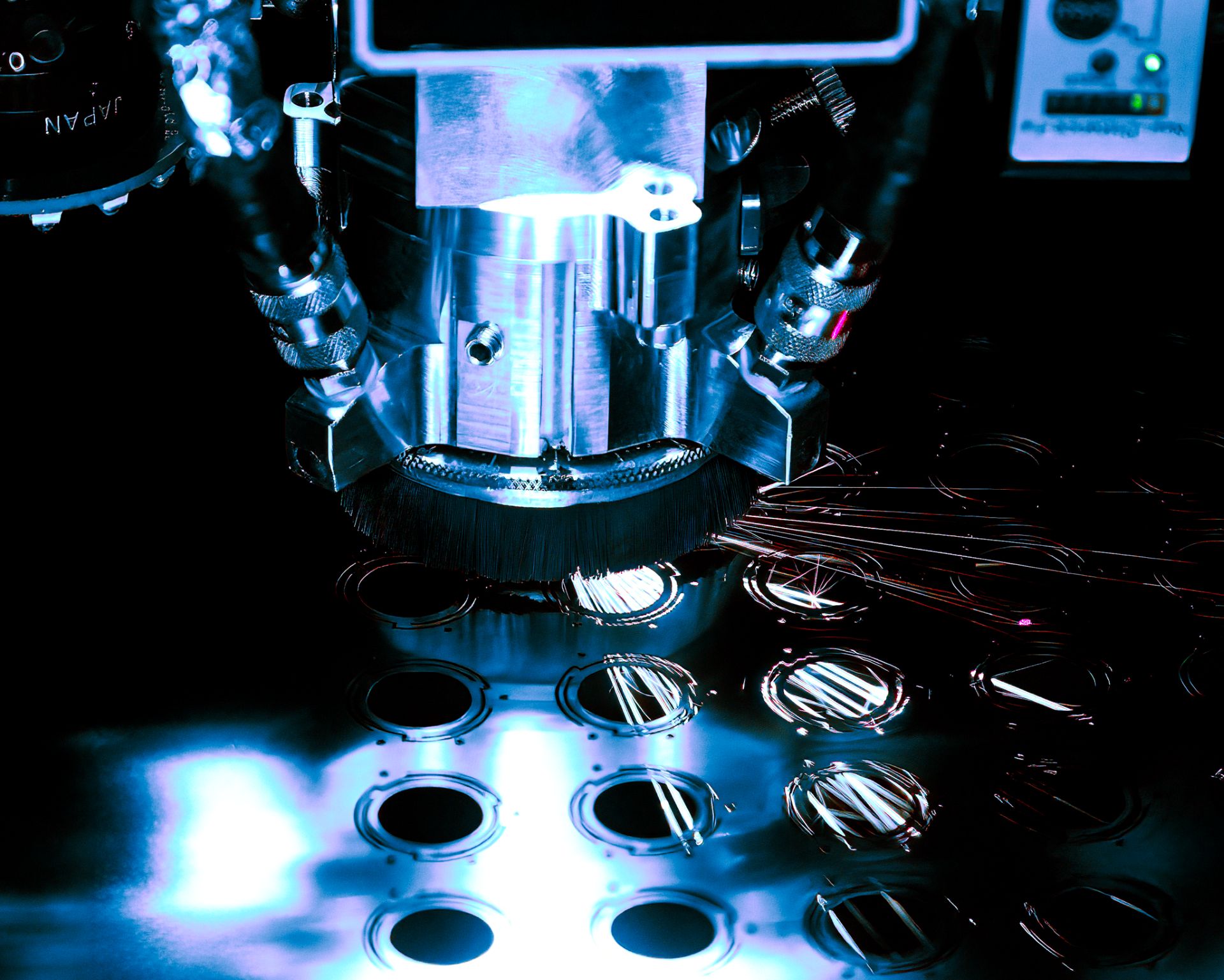
Fiber Tech: Best at cutting metal alloys in the range of 0.254mm up to 10mm thick, depending on the fiber lasers power. These are robust lasers capable of supporting production runs of flat sheets of alloys.

Lasers of course are not the only method supporting the semiconductor industry and though the bias for this content highlights laser technology, it does not mean that each of the other techniques does not have advantages. Understanding what each process can offer will be left to the engineers to compile and determine their best course of action.
Supporting the semiconductor industry in any aspect is a welcomed addition to manufacturing and laser cutting of challenging materials solidifies the relationship with engineering groups covering the multifaceted world of high-end chip manufacturing. With the constant push for products to be faster and more efficient, semiconductor research will continue to be a key influence on advanced technologies, but also on the world economy.
