Tips For Having Your PCB Depaneled By Laser Technology
The printed circuit industry never sleeps as electronics manufacturing is in constant demand and is especially true for the quick turn, high mix, and low volume service providers. They can range from just a few manufacturing lines to those larger companies hosting multiple buildings with multiple lines in each, working in some cases, 24/7. These demands to produce newly assembled electronics are part of the culture and industry make-up and include entities from manufacturing the PCB substrate, to chemical providers, to parts and components acquisitions and supply, to surface mount stencils, and depaneling specialists. These and others are part of a complex supply chain that relies on each other for support. Laser technology is used often for the manufacturing of metal mask stencils and is growing in popularity for use in the depaneling of the assembled PCB panels. This focus will be on tips you can use to streamline the process of working with laser depaneling specialists.
The Push for Laser Technology
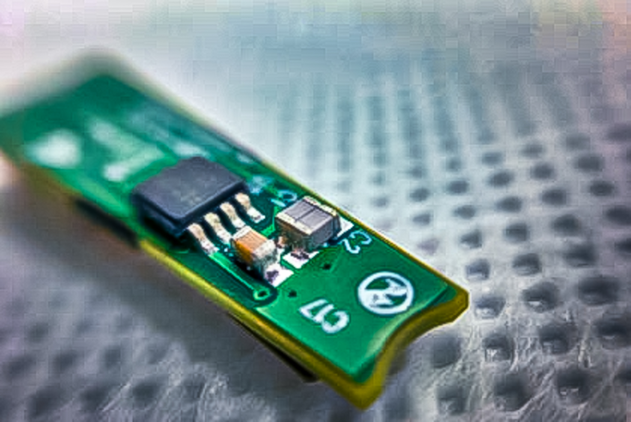
The PCB assembly industry has used for many years, mechanical routers, and this method has been successful, but for smaller and more delicate components, it can be detrimental. The nature of a router bit, even of the smallest diameters, does inflict stress and vibration onto the assemble panels. This unwanted impact can cause delamination and parts failure along with solder joints being broken. A solution to this problem that is more often seen on smaller board assemblies, is laser depaneling. Laser cutting machines, of the UV wavelength, work best to cut PCB’s out of FR4 and polyimide materials and can do so in thickness of just a few mils up to .120” or even thicker. Laser cutting is a non-contact method that has opened many new opportunities for pcb board design and electronics that traditional mechanical depanel techniques could not support. When seeking the expertise of a laser cutting service provider, keep these tips in mind:

- Data Is Key: The lasers will use the CAD data of board design. This will be the Gerber files or even an AutoCAD dxf or step files. The important layers needed will be fab drawing, drill layer, top and bottom layers. The data will need to be in the same panel form as the assembled boards. A single board layout is possible to use but will not be as accurate.
- Fiducials for Accuracy: To key in the X and Y coordinates, panels fiducials work best, with 3 locations being good, but 4 is excellent. Fiducials shapes that are round at about 0.5mm to 1.0mm in diameter are best and most common. However, cross shape fiducials will work as well. For boards that are missing fiducials, alignment may be done keying off vias or other points of data that can be seen on the board and data package.
- Component Locations: Assembled PCBs come either single or double sided. For double sided panels, a fixture is highly recommended. This ensures the panel lays flat during the cutting process. Fixtures can be made from ESD safe materials and returned to the customer or stored for future runs. Laser accuracy has cut boards with components as close as 8-10 mils to the board edge, making the method highly regarded for projects.
- ESD Safety: ESD is a concern for the electronics industry and having an ESD safe facility for any third-party support is vital. Your laser service provider should have ESD procedures and standards in place.
- Inspection Level Required: Inspection of the cut boards is a critical part of the laser depanel process. Measuring the cut profile to ensure it is within tolerance and inspection of the cut edge to confirm accuracy and that no components were damaged. The level of inspection depends on the needs of the project and can be from AQL levels to 100% or some other agreed upon interval. Laser providers will use OGPs (Optical Gaging Products), visual comparators, or some other measuring devices. Ask what types of system are used and what levels of inspection are offered.
- Pre and Post Laser Handling: Packaging of sensitive and often costly board assemblies is important to keep in mind. The use of ESD safe packaging materials in sturdy enclosures for shipping too and from your service provider prevents damage. Some examples of this are: ESD safe foam, Gel-Paks, custom trays with lids, ESD safe bags.

The diversity of projects being manufactured by the electronics industry changes constantly, perhaps hourly at very active manufacturers and the requirements for quality and precision are at constant high levels. Working with qualified providers is the best way to continue the integrity of the supply chain.
Conclusion
In conclusion, adopting laser depaneling for your PCB assembly can significantly enhance the quality and precision of your projects. By paying close attention to data accuracy, fiducial placement, component handling, ESD safety, and thorough inspection, one can ensure that the transition to laser technology is smooth and successful. For those new to this field, these tips serve as a guiding framework that can help navigate the complexities of laser depaneling while achieving optimal results. Partnering with a knowledgeable and reliable laser service provider is essential in maintaining the highest standards and integrity of your electronic products.
