Laser Cutting Services for Semiconductor Manufacturing
Laser Cutting Semiconductors
Semiconductors are fascinating devices developed over many years of research and development. This progress of advanced electronics has not been the sole accomplishment of the semiconductor industry, as such complex and highly technical components and processes are needed to create them. Partnering with a wide range of manufacturing disciplines, the semiconductor industry has created supply chains that give the best in capabilities and one of those is laser cutting technology. Semiconductor laser cutting supports the industry by providing precision components to multiple manufacturing sectors along with support for these with product development and volume production support. With competition between other methods, laser cutting has become known for its expertise in processing thin films and materials used in the production of components used in semiconductors. This capability was not given but earned through providing the necessary levels of quality and commitment to strict procedures and protocols that the semiconductor industry requires. An example of this is laser cutting polyimide for chip packaging and PCB substrates. Let’s learn the process of this and in other important ways how laser cutting provides services to semiconductor manufacturers.
Engineering Support
The direction to use laser manufacturing often is supported by engineering teams that can be working from mechanical, electrical, and process groups. The goals of the team in the semiconductor industry are to develop and promote the advancements of their technology. By doing so, our products and ways we communicate, travel and receive care are just glimpses of how semiconductors influence our quality of life. Laser cutting plays a crucial role across various sectors of the semiconductor industry due to its unparalleled precision, minimal heat-affected zones, and ability to process delicate and diverse materials. Engineering teams working in the industry have discovered for the past few decades the advantages of using laser technology to advance products and processes. Here’s a breakdown of the kinds of materials being laser cut and why:
- Silicon (Si)
- Low K dielectric
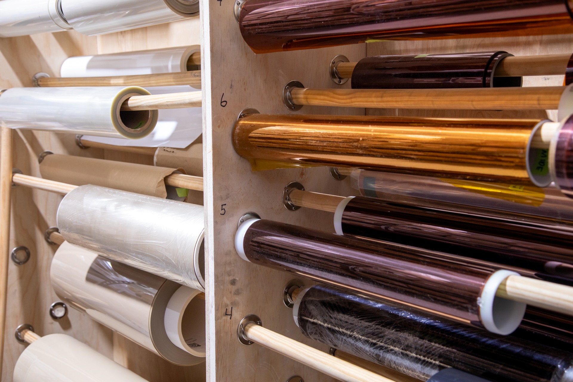
- Thin Films and Adhesives
- Metal Alloys: Stainless Steel, aluminum, copper, titanium, nickel, tungsten, others.
- Plastics and Polymers: Acrylic, POM (Delrin), Polyimide (Kapton), polypropylene.
- Gasketing Materials: Graphene, Q-Pad, and other gasketing materials.
Taking new ideas forward are what engineers provide and to support this development and keep existing production flowing, laser cutting specialists work closely with engineering teams to accomplish their goals.


Advantages To the Semiconductor Industry
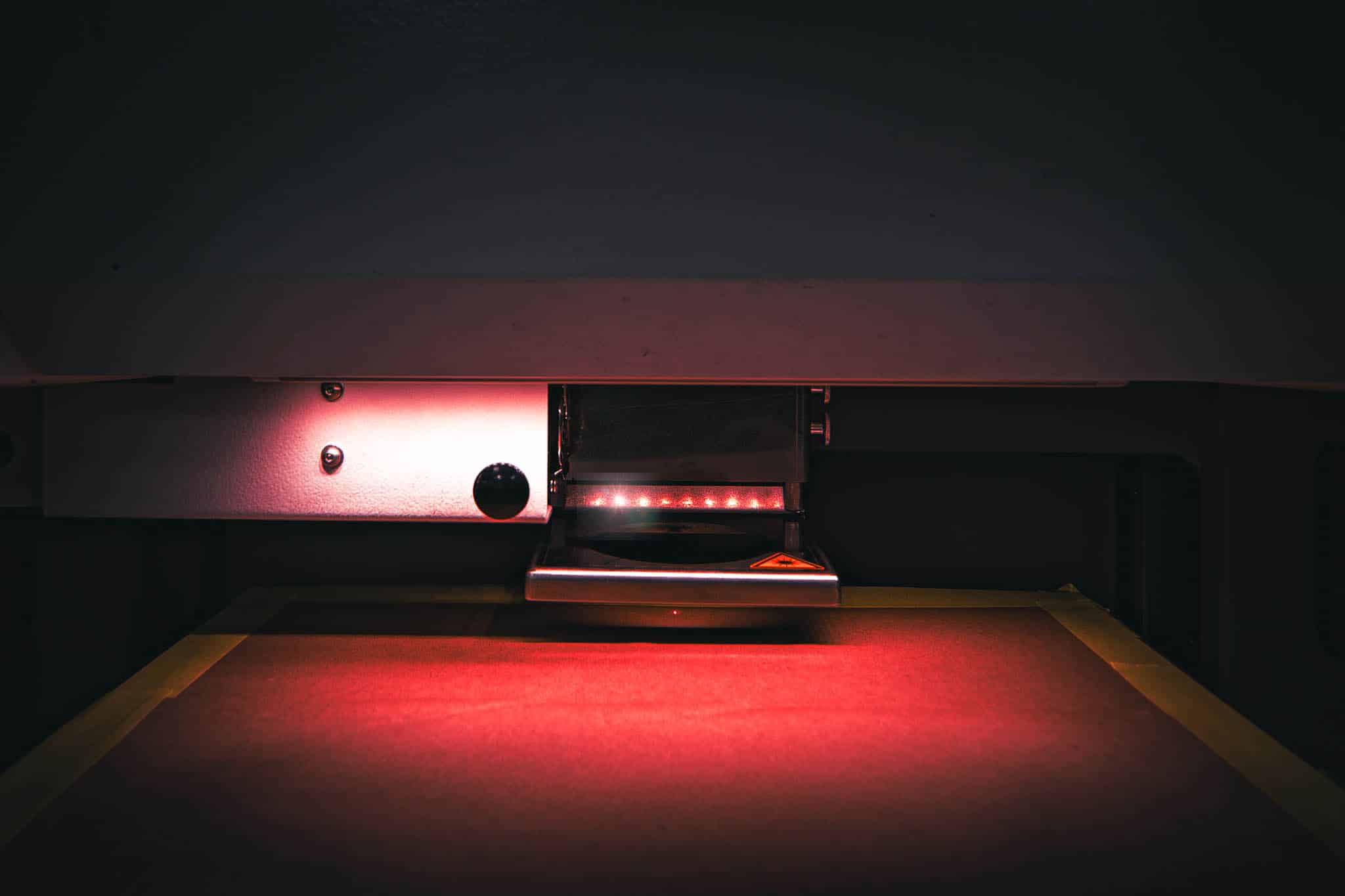
Laser technology has a keen advantage over many other methods that it does not incur cost for special tooling or extensive set-up. The parameters and process are catalogued and stored as the “laser tool”. These tools are then locked in and can rapidly take a development project into a production phase. This flexibility comes from the use of multiple platforms that encompass laser systems such as ultraviolet and fiber lasers. Each of these systems has unique capabilities and materials that they can cut and by doing so they stand out as key methods for providing precision laser services. Listed below are some key aspects of ultraviolet and fiber laser lasers used in support of semiconductor parts.
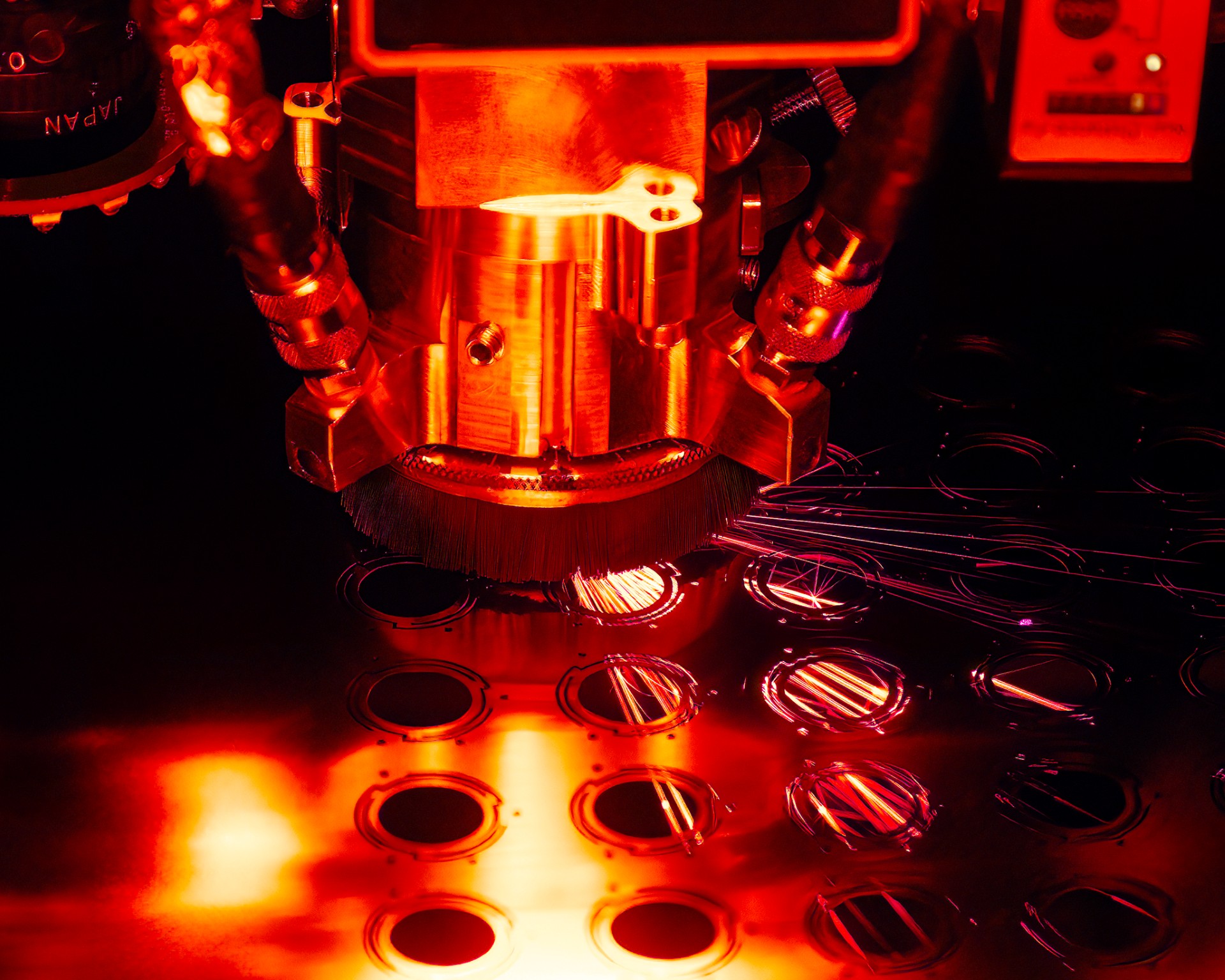
UV Laser Technology: Best at ultra-thin metal foils and sheets in thickness range of 0.0127mm to 0.254mm. Also excellent with polymers, gasketing materials, precious metals, adhesives and materials sensitive to physical and thermal damage. Also used for many R&D and production manufacturing. UV lasers, compared to fiber, are low powered and rely on their ability to process in a series of laser passes. As mentioned earlier the parameters set forth are called the “laser tool’. A great advantage to this is that any changes to the design requirements, other than the material, will only need an adjustment tov the CAD (Computer Aided Design) file. UV lasers are capable of cutting to tolerances held as tight as +/- 0.0127mm to 0.0254mm.


Fiber Laser Technology: This system type is excellent for cutting metal alloys in the range of 0.254mm up to 10mm thick, depending on the fiber lasers power. These are robust lasers capable of supporting production runs of flat sheets of exotic alloys to stainless steel and aluminum. These systems also cut in a series of laser passes and hold tight tolerances of +/- 0.0254mm.
Specialized Components
Laser cutting specialists working in support of the semiconductor industry are being asked to process materials in ways that can be more challenging for other mechanical methods like CNC machining, die-cutting, and stamping. The advantages of using laser cutting for chip packaging, for dielectric and insulating layers, to substrates for flexible circuits are some of the ways laser technology is being used. The advantages of semiconductor laser cutting over mechanical means for crucial components give engineers options for new designs and materials. Materials are always at the forefront of manufacturing, as in many cases, there will be one specific material that outperforms other similar types. With clean and debris free components being critical to many aspects of semiconductor devices and assemblies, cleanroom laser processing has been a must. You will find components being made such shown below:
- Dielectric and Insulating Layers: Polyimide’s excellent electrical insulation properties and low dielectric constants make it an ideal material for creating insulating layers between different metal interconnects within a chip package.
- Stress Buffer Layers (Passivation Layers): Polyimide can act as a buffer to absorb stress. Semiconductor devices are sensitive to mechanical stress that can occur from differences in thermal expansion coefficients between the silicon chip and other packaging materials.
- Gaskets for Processing Equipment: Gasketing materials like Grafoil and Q-Pad are used in the processing of wafers.
- Lead Frames and Interconnects: Copper is a go to choice for these types of parts.
- Tooling and structural needs: Stainless steel and aluminum are used.
- Adhesive and Bonding Layers: The die attach process can use polyimides with adhesive films for bonding chip components.
- Substrates for Flexible Circuits (Chip-on-Film – COF): Applications requiring flexibility polyimides are the base substrate for flexible printed circuits. For Chip-on-Film (COF) technology, the use of polyimides opens the door for compact and flexible packaging solutions.
- Encapsulation: Using polyimides to protect sensitive components from moisture, chemicals, and mechanical impact or other environmental factors.
Producing these types of parts needs the expertise of laser cutting providers to select the best laser cutting machines to match the capabilities that specialize in cutting materials. This becomes a great advantage to manufacturing in solving challenges.
Material Highlight: Grafoil and Q-Pad
Grafoil and Q-pad are used very extensively in semiconductor processing equipment and the integrity of these precision tools are vital in the production stream. The uniformity of the cut profiles for parts ranging in size from 11.500” inches OD x 9.75” ID to 19.600” ODx17.75” ID, are made to tolerances as small as +/- 0.0254mm. Shims can be vital in the functioning of mechanical devices. Requiring more durability, shims from stainless steel reinforced Grafoil, have proven to be a key part of the laser services provided for both R&D and long term production.
Why Use A-Laser for Your Semi-Conductor Material Needs?
The demands of high quality, tight tolerances, and reliable performance are capabilities that laser technology has. For semiconductor laser cutting these additional characteristics add even more advantages that can ultimately lead to using these non-contact methods of manufacturing. Keep these factors in mind when considering the manufacturing needs of your next component:
- Minimized HAZ: UV lasers cut into a series of passes designated by scan fields. The number of scan fields and passes varies per the design, thickness and material. These are then programmed to eliminate or minimize any HAZ or heat-affected zones.
- Rapid Throughput: Laser Cutting is a no contact method, so there are no fixtures or cutting dies required. Two main elements are needed, which are the CAD and material.
- Product Development: R&D and prototype needs is much faster than other methods. Iterations do not incur cost for new tooling but just require a change to the CAD.
- Materials Other Cannot Cut: Sourcing a supplier that has the capability of processing a wide range of materials is a big plus for procurement managers. For the thin and ultra-thin materials used for semiconductor manufacturing, laser cutting can easily cut metal alloys and quickly be set to cut non-metallics like polymers and gasketing materials, without extensive set-up.
Laser cutting technology is revolutionizing semiconductor manufacturing by offering unmatched precision, versatility, and efficiency. From ultra-thin materials to robust metal alloys, the non-contact methodology enables engineers to meet stringent industry demands while minimizing heat-affected zones and maximizing throughput. Whether for rapid prototyping or high-volume production, laser systems deliver consistent and reliable results across a diverse range of materials. Explore how advanced laser cutting services can elevate your semiconductor projects, meet complex requirements, and drive innovation in your designs and processes.
