Material of the Month: FR-4
FR-4
FR-4 materials are widely used in PCB manufacturing. Outside of direct production, its material structure isn’t too well known.
The NEMA designation is the route of its code-name. The initial part “FR” is short for Flame Retardant. This designation was created in 1968 by NEMA. FR-4 relates to a class of materials that fit the definition rather than one individual material.

What is FR-4?
In this context, we will use FR-4 as a generic name for “prepreg” materials that fit our previously mentioned standards. Prepreg being pre-impregnated materials. Usually, these consist of a woven glass fiber material set with epoxy resin.
How are PCBs constructed?
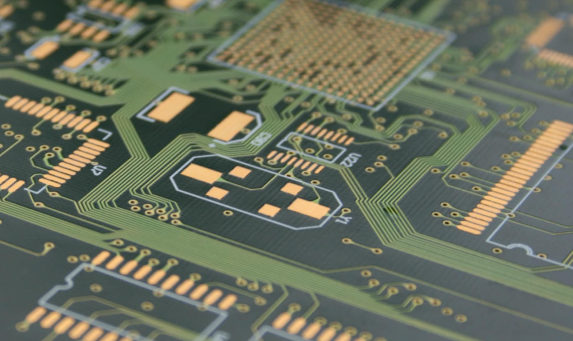
A PCB or Printed Circuit Board is simply an electrical circuit that has been flattened down and contained within layers of FR-4. By replacing wires and cables with copper tracks we can drastically reduce the overall size of the circuit. These tracks are cut from a single sheet of copper. In order for these tracks to cross one another without shorting, we can create multiple layers with a layer of FR-4 separating them. If PCBs were sandwiches, copper would be the meat and FR-4 the bread. Multi-layer PCBs would be more like a club sandwich.
Why is FR-4 suitable for PCB production?
High strength to weight ratio combined with close to zero water absorption and very strong insulative properties make it suitable as housing for complex circuits to be constructed within discrete layers. Its low thermal conductivity helps prevent overheating of sensitive components.
A-Laser PCB Depaneling
How does it work?
Our high-precision lasers operate at a wavelength of 355nm which is in the UV spectrum.
When selecting the correct laser for a specific operation one must consider the light absorption rates for different materials. For example, cutting stainless steel we can see that the absorption peaks in the IR range at 1,064nm (from Nd:YAG fiber lasers) and at 10,640nm (C02 lasers).
The compound layers of PCBs all lean towards good absorption in the UV spectrum. copper, glass fiber, and epoxy will all be cut by a concentrated UV laser source. This will occur at different speeds for each instance. To optimize for this we can laser parameters such as frequency, power, and spot size along with scanner settings of speed, hatching, and repeats can be altered to optimize the cut quality.
Although laser is the best choice for precision the robust nature of PCBs does make depaneling somewhat slow. The best option for fast accurate depaneling is a combination of routing with laser. This routing can be done way ahead of the component addition.
Why use our depaneling services?
Our go-to choice of technology is always laser. So we are biased, yes but we can back it up. There are many methods to depanel PCBs including mechanical routing, scoring and sanding, punching, and many more. Our laser-controlled operations are fully contained within individual enclosures trapping and removing any byproducts of the separation. Laser depaneling offers smaller geometry tracing when compared to milling or routing, better accuracy compared to punching, scoring, and sanding. Above all, laser technology gives outstanding repeatability.
Our expert engineers will ensure that each board is within spec and exactly what you need.
